Glass Carrier Wafer and Glass Carrier Panel

High-performance glass carriers for advanced semiconductor packaging

For decades, SCHOTT has built a leading reputation for high-quality glass carrier wafers and panels, serving advanced industries like semiconductors, optoelectronics, automotive, science, and biotechnology. Our experts help develop tailored solutions to meet specific customer needs.

What are glass carrier wafers?

Glass carrier wafers are precisely manufactured discs made of thin glass materials such as borosilicate and alumino-borosilicate. These materials are selected for their excellent thermal expansion properties and transmittance. Manufactured using advanced technology, the wafers meet stringent quality standards and are tailored to suit the specific requirements of the industry.

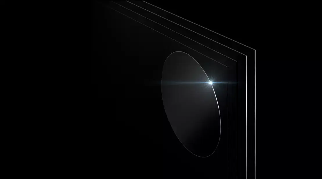
Why choose SCHOTT glass carriers?

Our glass carriers are essential in semiconductor applications as temporary bonding and debonding substrates for silicon wafers and dies. SCHOTT glass with high optical transmission – from UV to IR – enables efficient laser-assisted debonding and advanced packaging solutions.

As semiconductor architectures become more complex, demand for ultra-flat, mechanically and chemically stable carrier materials continues to grow. Glass wafers and panels are widely used in 2.5D and 3D ICs, fan-out wafer- and panel-level packaging (FOWLP/FOPLP), and wafer thinning applications.

Glass carrier highlights

High raw glass quality

High reproducibility of our melting processes ensures high and consistent quality of raw glass. Our strict process controls guarantee stable material properties — giving you a reliable foundation for every step of your semiconductor manufacturing process.

Designed for semiconductor processes

Our glass carriers are ideal for temporary bonding, silicon thinning, and fan-out packaging. With state of the art processing capabilities, we meet diverse semiconductor requirements for both carrier wafers and panels — across all relevant formats and dimensions.

Versatile processing options

State of the art processing capabilities are available to meet diverse semiconductor requirements for carrier wafers and panels. Our broad material and geometry portfolio ensures the right solution for your specific application and process environment.

Process-ready design

Laser-marked, cleanroom-packaged traceable wafers and panels enable seamless integration into high-tech manufacturing. Each carrier is inspected and packaged under ISO 5 conditions — ensuring full traceability and process readiness from delivery onwards.

Glass carriers produced to industry standards

Ultra- and megasonic cleaning is performed in ISO 5 cleanroom conditions. Inspection and packaging take place in FOSB and RTU wafer boxes under ISO 5 conditions — meeting the highest standards for cleanliness and handling in semiconductor environments.

Technical expertise

Our specialists offer tailored support to help customers find the best carrier material for their application. From initial material selection to process qualification, we accompany you with application know-how and hands-on technical guidance throughout.

Broad choice of materials for glass carrier to fit customers requirements

SCHOTT glass portfolio with a broad CTE range to meet customer device materials due to our broad choice of materials we can fulfil our customers requirements.
Graph showing the CTEs of a variety of SCHOTT glasses

Geometrical properties of SCHOTT glass carrier

Item Wafer(1) Panel(1)
Format  6", 8", 12" [150–300 mm]  max. 650 × 650 mm(2)
Thickness(3)  0.40 – 2.75 mm  0.50 – 2.75 mm
Thickness tolerance(4)  ± 2.5 – 5.0 µm  ± 15 – 20 µm
Total thickness variation (TTV)(4)  ≤ 0.5 – 2.0 µm  ≤ 15 – 20 µm
Warp(4)  12": ≤ 50 µm
 8": ≤ 30 µm
 ≤ 100 – 200 µm
Cosmetic quality Scratch/Dig  40/20 – 20/10  40/20 – 20/10


(1) Tighter specifications upon request
(2) Typically 600 x 600 mm
(3) Typical values, other thicknesses on demand possible
(4) Typical values, depending on glass type and thickness

Bonding and debonding of glass carrier

High UV transmittance allows temporary bonding and debonding
Graph showing the optical transmission of SCHOTT Glass Carriers

Spectral transmittance: thickness 1.1 mm for λ = 250 nm to 400 nm

Graph showing the optical transmission of SCHOTT Glass Carriers200-500 nm-EN

Spectral transmittance: thickness 1.1 mm for λ = 200 nm 500 nm

SCHOTT glass carrier can be delivered as follows:

  • Flat/notch: According to SEMI standard
  • Laser marking: According to SEMI standard, T7, QR-Barcode/unique number
  • Cleaning: Ultra/mega-sonic cleaning and cleanroom ISO 6
  • Packaging: Inspection and packaging under ISO 6 in wafer boxes (FOSB, RTU, etc.)

Want to know more? Let’s talk

Whether you need more information, samples, a quote, or advice for a project, we would be delighted to talk to you.

Contact us
Man in glasses in business office on phone while working on laptop_605x350.jpg